
In this article, the CMOS Logic is explained, and how to design different logic gates using CMOS logic is explained in detail.
What is CMOS Logic ?
If you see any logic gate then its characteristics like its voltage levels, fan-out, speed, power consumption depends on the technology which is used to design these logic gates.
There are different logic families like RTL, DTL, TTL and MOS, ECL logic family. Some of them are already obsolete, and are not used in the design these days. While some of the logic families like TTL, ECL, MOS and CMOS logic families are quite popular and widely used in the digital circuits.
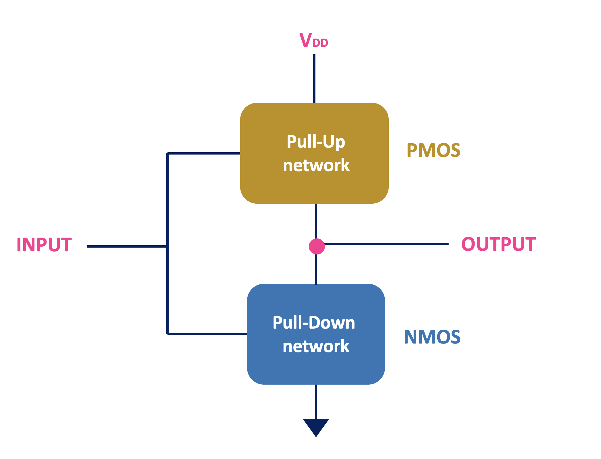
CMOS stands for Complementary Metal Oxide Semiconductor. And CMOS based logic gates uses complementary pair of NMOS and PMOS transistors. When MOS transistors are used as logic gate then they are used as a switch.
In both NMOS and PMOS transistor, the voltage applied between the gate and source acts as a control voltage.

By controlling the gate to source voltage, PMOS and NMOS transistor can be used as a switch. And they can be used to design a logic gate.

CMOS logic uses both NMOS and PMOS transistors. The PMOS transistors are used as pull-up network and NMOS transistors are used as pull-down network. And because of that, the static power consumption of the CMOS based logic gates and logic circuit is very low compared to the logic gates which is designed using only either NMOS or PMOS transistors. Moreover, CMOS based logic gates has higher noise margin compared to NMOS and PMOS based logic gates.
NMOS Inverter and the Issue of Power Dissipation with NMOS and PMOS Transistors
Using just either NMOS or PMOS transistors also, it is possible to design a logic gate. The basic design of NMOS inverter is shown below.
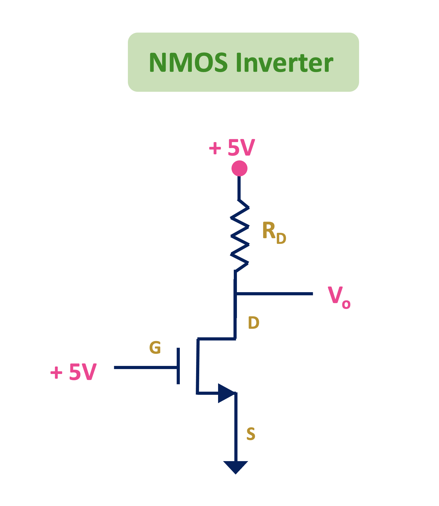
Let’s assume that the threshold voltage (VT) of the NMOS transistor is 0.5 V. When VGS = 5V or when VGS > VT , (Let’s assume that logic ‘1’ is 5V) then MOSFET will be ON and acts as a close switch (Ideally, the ON resistance of the MOSFET is 0 ohm) And the output will get connected to the ground. But actually, there will be some finite ON resistance of the MOSFET (10s of Ohm). And the drain resistor RD is in kilo-ohm. Therefore, in actual case also, the output will be very close to 0V or logic ‘0’.
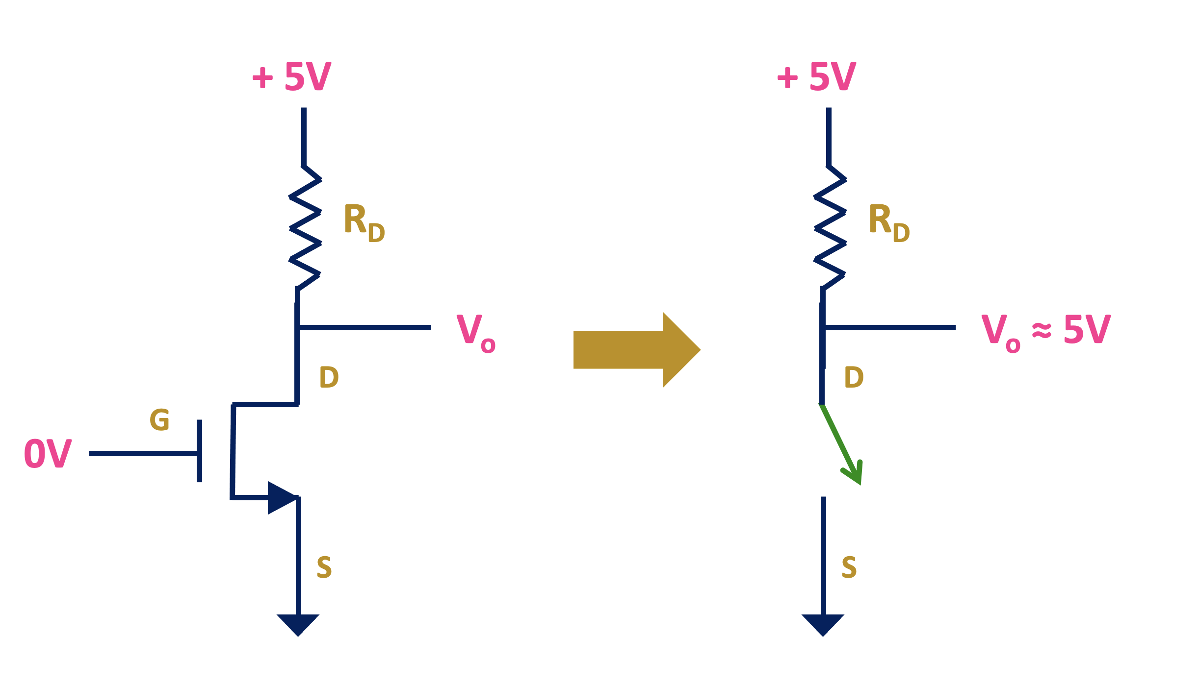
Similarly, when VGS = 0V or logic ‘0’ then MOSFET will be OFF and it will act as a open switch. And through the drain resistor, the output will get connected to the supply voltage. That means when input is 0 then output is VDD.
And in this way, this circuit will act as an inverter.
Now, when we are designing this logic gate using a discrete components, then it is possible to include large drain resistor in the circuit. But in the integrated circuits, it is difficult to fabricate a resistor with a large value.
Therefore, in the ICs, instead of resistor, the MOSFET is used as an active load.
As shown below, the gate and drain terminals of the MOSFET are connected to VDD. That means the upper NMOS transistor remains in the ON condition. And in the ON condition, its ON resistance will provide the required drain resistance for the Lower NMOS transistor.

Of course, by changing the MOSFETs device parameters, it is possible to ensure that, its ON resistance is in kΩ.
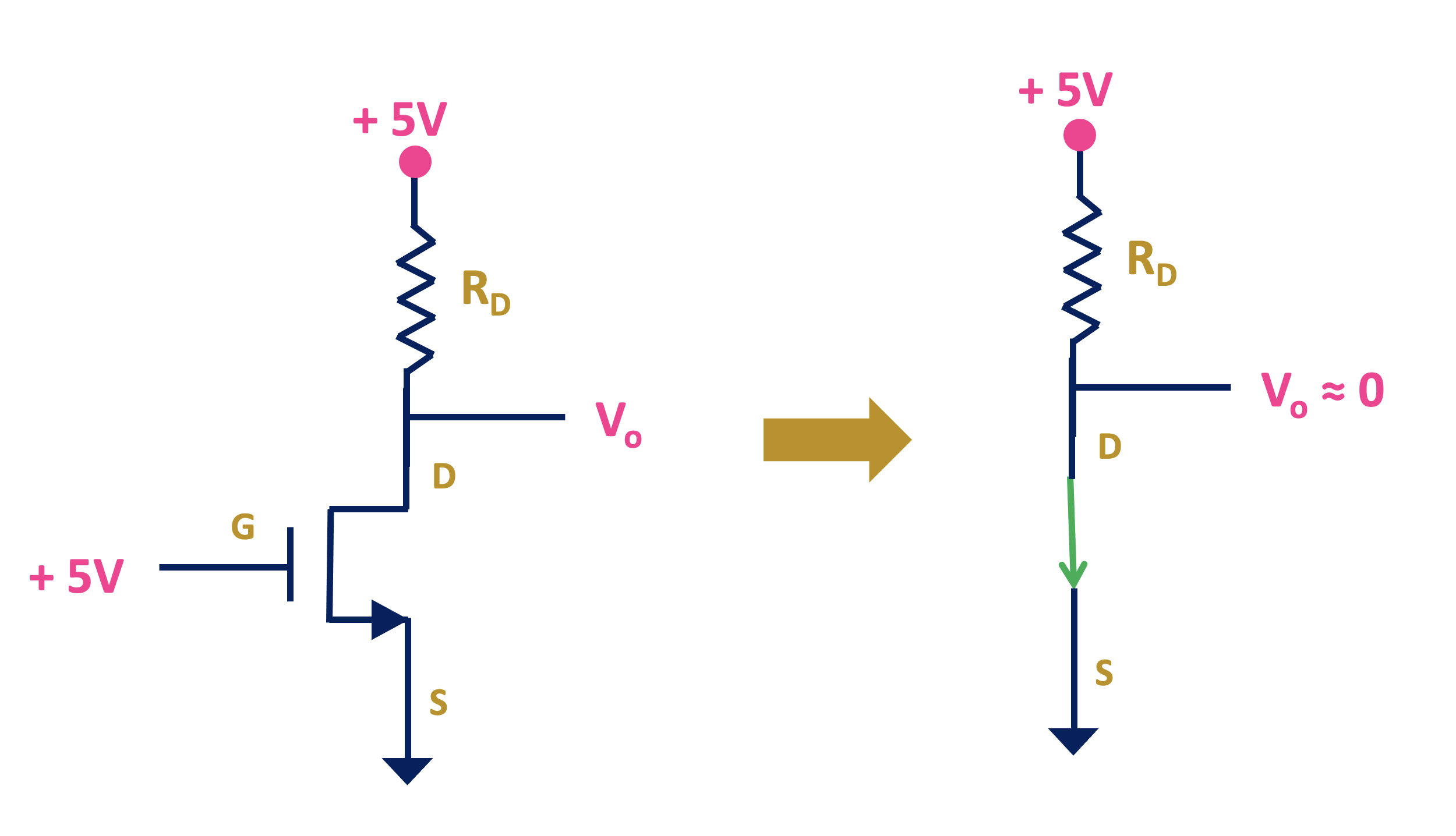
The issue with this design is that, there is a static power dissipation across the transistor.
For example, when the input to the inverter is ‘1’ then NMOS will be ON, and it provides very low resistance. And because of that, there is power dissipation across the NMOS transistor.
That means, if the input to the inverter is a clock signal which is continuously changing between ‘1’ and ‘0’ then for half of the total time, there will be a static power dissipation across the NMOS transistors.
And the same is case with the logic gate designed using PMOS transistors.
That means when we are designing the logic gates only using NMOS or PMOS transistors then there will be a static power dissipation. And the power dissipation becomes a critical factor when there are millions of such transistors in the circuit.
NMOS passes weak logic ‘1’ and Strong logic ‘0’
Apart from the power dissipation, the other issue with the NMOS transistor is that, it passes weak logic ‘1’.
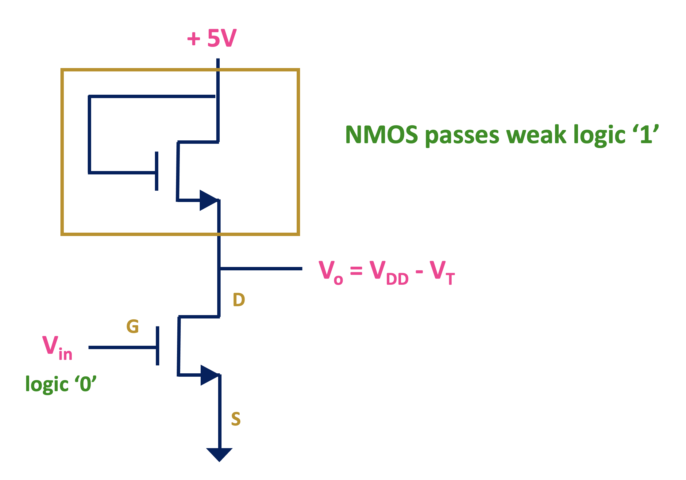
When the input to the inverter is logic ‘0’, then output of the inverter should be high and ideally, it should be equal to VDD. But actually, here the output will not go beyond VDD – VT.
Because, if output of the inverter goes to 5V, then the source terminal of the upper NMOS transistor will be at 5V and therefore, VGS will become 0V.
Now, for MOSFET to be in ON condition, VGS should be more than VT. That means in this case, the voltage at the source terminal of the upper MOSFET won’t go beyond VDD – VT.
Otherwise, the upper NMOS transistor will become OFF.
So, for example, if threshold voltage of NMOS is 0.5V and supply voltage is 5V then output will not go beyond 4.5 V.
That means we will not get full voltage swing. Or in other words, NMOS is weak to pass logic ‘1’.
But at the same time, NMOS transistor passes strong logic ‘0’.
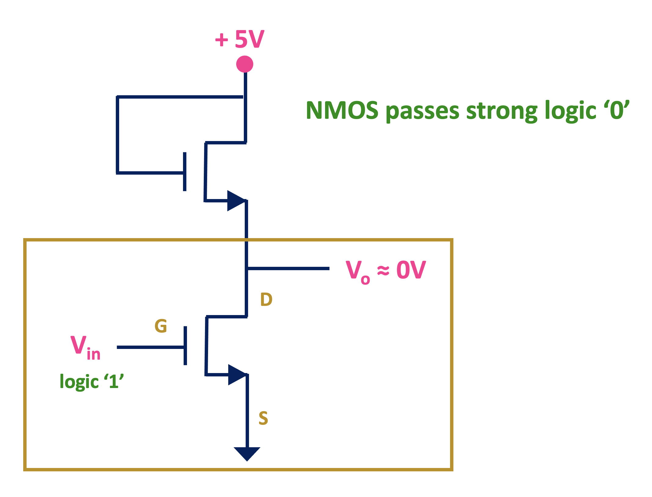
For example, if the input to the inverter is logic ‘1’ then NMOS will be in the ON condition and since source is connected to the ground, it will pull down the voltage of the drain terminal to 0V.
That means NMOS passes weak logic ‘1’ but it passes logic ‘0’. And it can be used in the pull-down network to pull down the voltage of specific node to 0V.
PMOS passes strong logic ‘1’ and weak logic ‘0’
As shown below, here the source of PMOS is connected to 5V and drain is connected to capacitor.
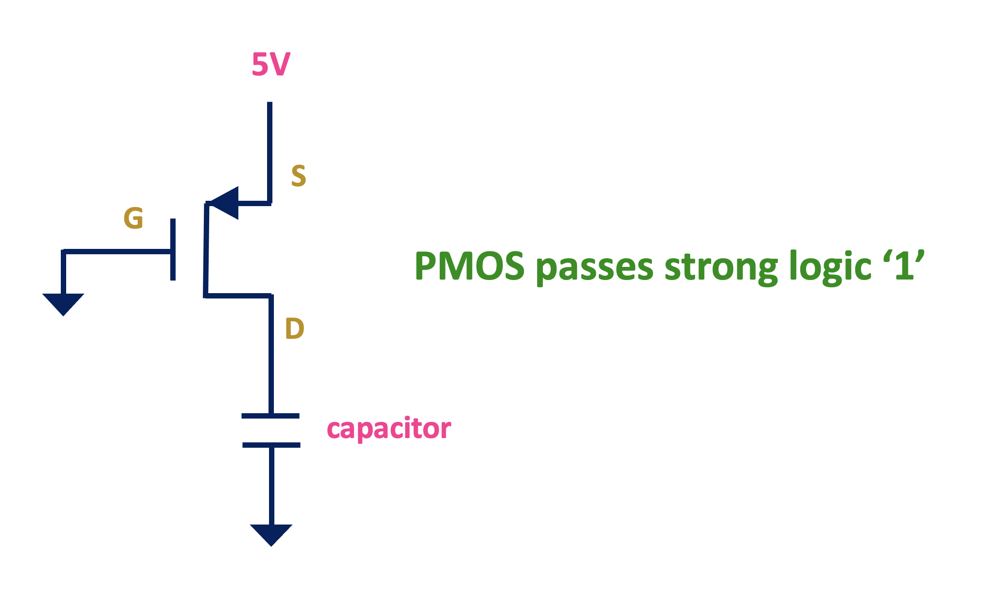
Now, when input to PMOS is 0V then VSG is more than VT and PMOS will act as a closed switch.
So, capacitor at the drain terminal will start charging towards 5V and eventually the voltage at the drain terminal will be equal to 5V.
So, when we want to pull-up the voltage at the drain terminal to the supply voltage, then we can use the PMOS transistors.
But PMOS transistor is weak for passing logic ‘0’.

Let’s say now the drain terminal is connected to ground. And capacitor is connected at the source terminal. And let’s assume that, initially, the voltage across the capacitor is 3V.
So, now when VG = 0V, then VSG is more than VT, and because of that, PMOS will conduct and it will try to bring down the voltage of the source terminal to 0V.
So, capacitor will start discharging. But as soon as the voltage at the source terminal reaches threshold voltage, then MOSFET will be turned off. Because now VSG = VT.
That means the voltage at the source terminal cannot go below threshold voltage.
So, for example, if the threshold voltage of the MOSFET is 0.5V then the voltage at the source terminal will not go below 0.5V. That means PMOS is weak to pass logic ‘0’.
And that is why it not preferable to use the PMOS transistor in the pull-down network. But it can be used in the pull-up network where we want to pull up the voltage of the specific node.
In the CMOS network both PMOS and NMOS transistors are used. The PMOS is used as a pull up network and NMOS transistors are used in the pull-down network.
And because of this configuration, there is almost no static power consumption in the CMOS logic gates.
CMOS Inverter
As shown below, PMOS transistor is used as a pull-up transistor, so its source is connected to supply voltage and drain is connected to the output node.
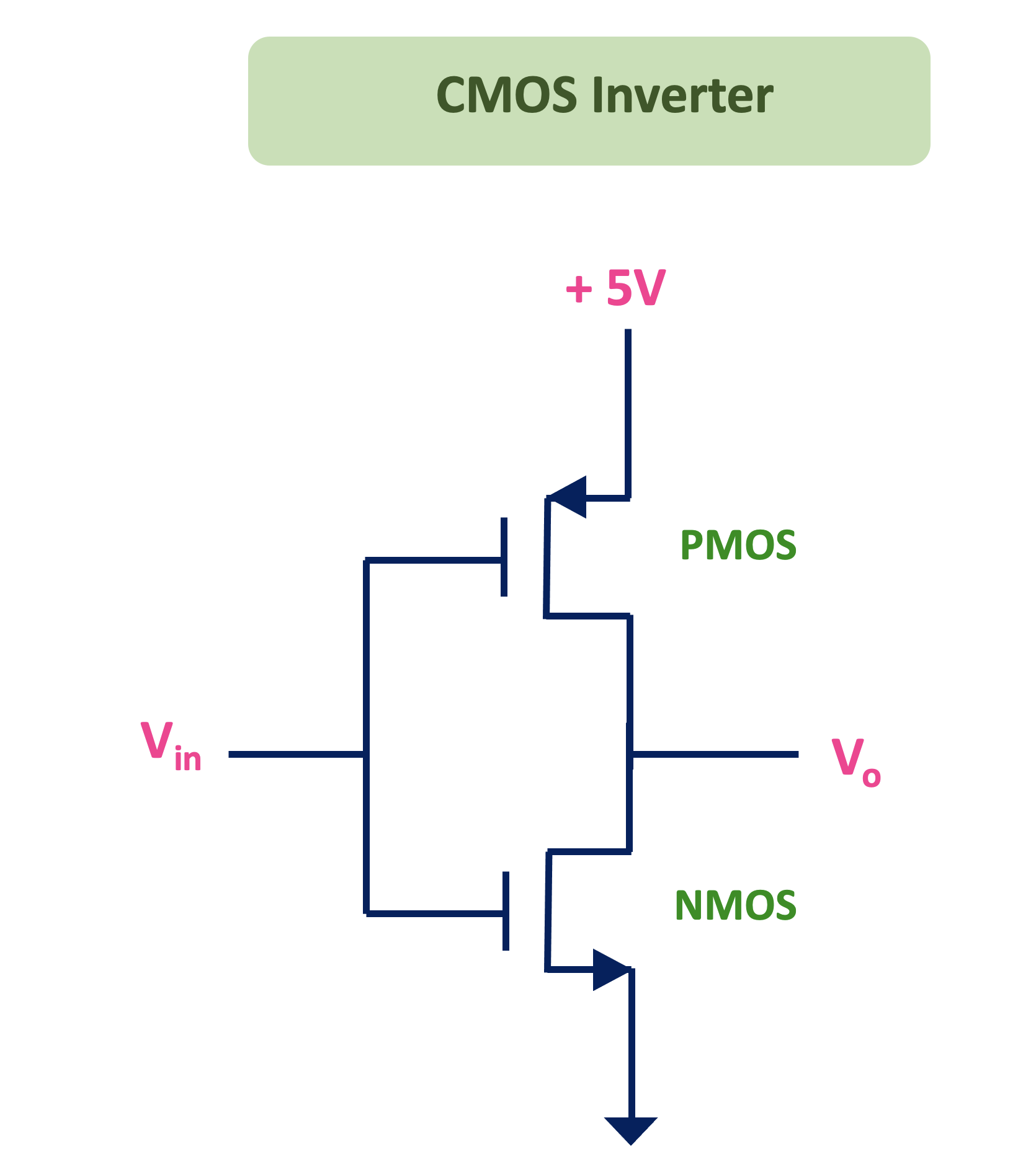
Similarly, the NMOS transistor is used as a pull-down transistor. That means its source terminal is connected to ground terminal and drain is connected to output node.
And the gate terminals of both PMOS and NMOS transistor is connected to the input.
Working of CMOS Inverter:
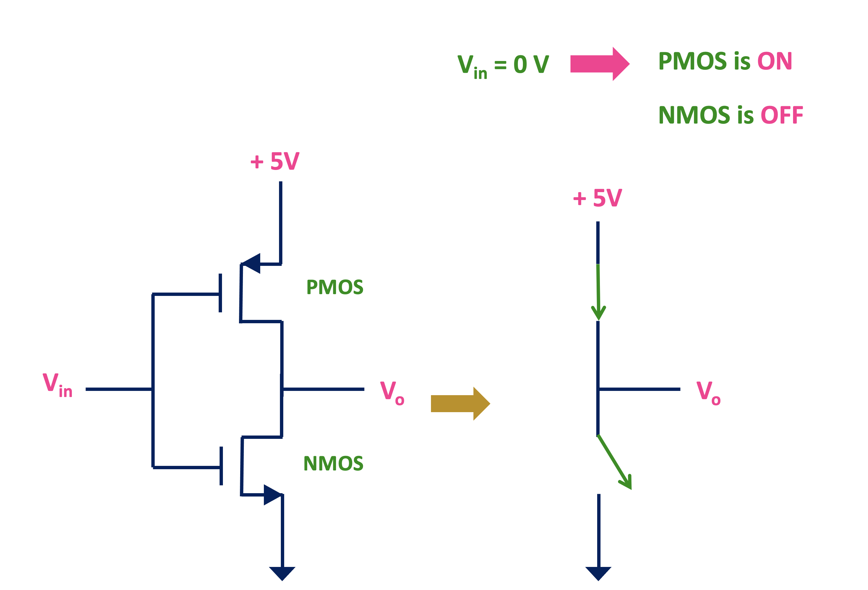
When input is low or logic ‘0’, then VSG > VT for this PMOS transistor and that’s why PMOS will be ON. On the other end, for NMOS transistor, VGS < VT.
that means when input is logic ‘0’, PMOS transistor will be ON and NMOS transistor will be OFF.
And that’s why the output will be connected to 5V.
Moreover, since PMOS passes strong logic ‘1’ , the output will be very close to supply voltage.
That means when Vin is logic ‘0’ then output is logic ‘1’.
On the other end, when Vin is logic ‘1’, then PMOS will be OFF and NMOS will ON.
So, in that case, the NMOS transistor will pull-down the output voltage to logic ‘0’. And since NMOS passes strong ‘0’, so output will be very close to 0V.
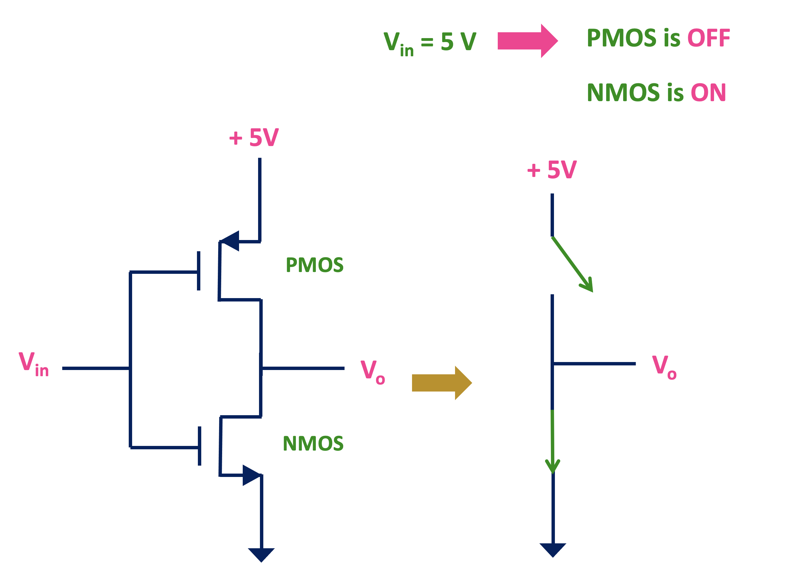
So, in this way, at any given time either PMOS transistor is ON or NMOS transistor is ON. And there is no direct path from supply to ground.
And because of that, the static power consumption of CMOS logic gate is almost negligible.
Implementation of Logic Gates using CMOS Logic
In general any CMOS based logic gate consist of Pull-up network and pull-down network. The pull-up network consists of PMOS transistors while pull-down network consist of NMOS transistors. And inputs to both networks are same.
So, we have already discussed about the CMOS inverter. Similarly, let’s see how to design other logic gates using CMOS logic.
Implementation of NAND and NOR gate using CMOS Logic:
NAND Gate:
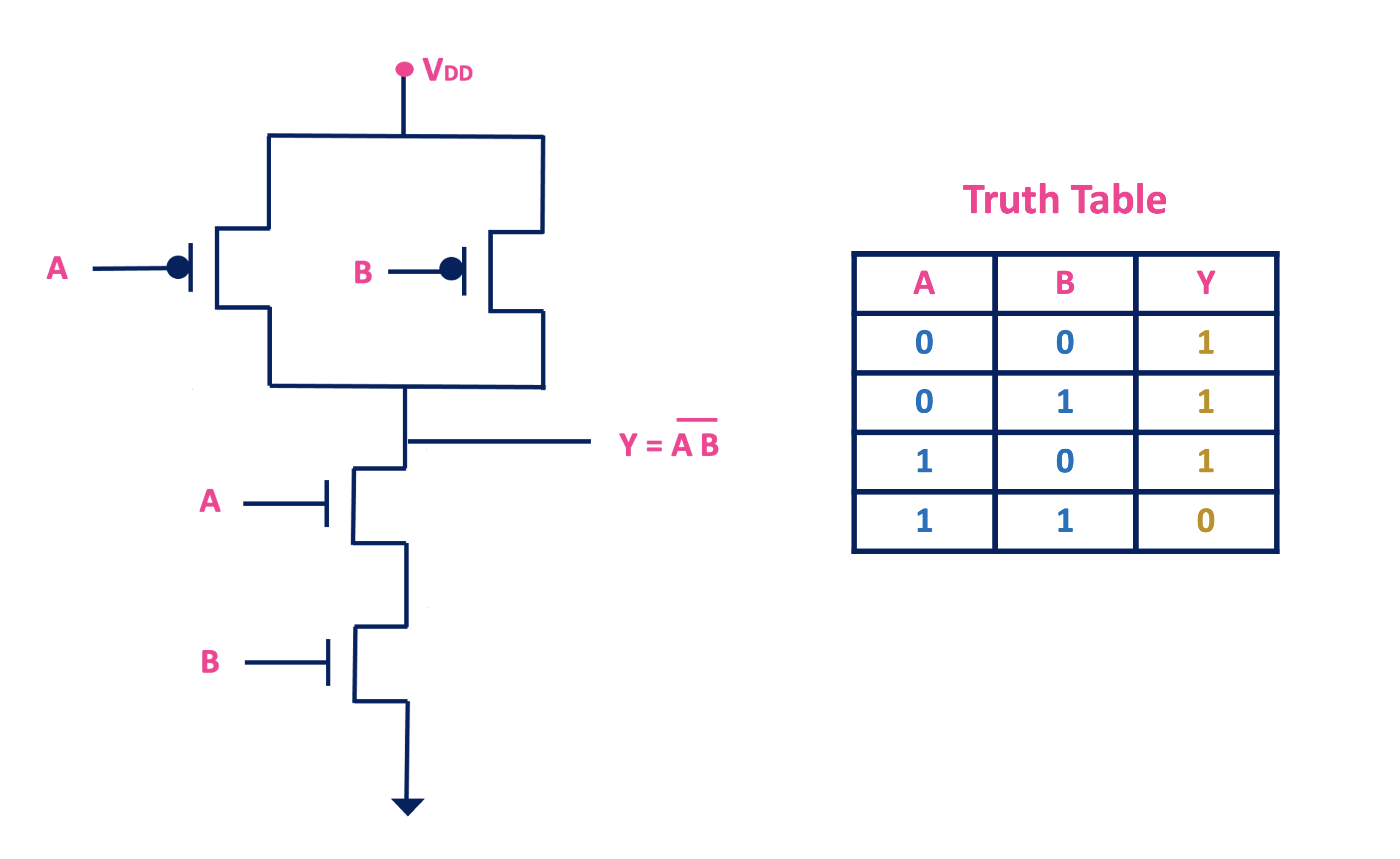
For two input NAND gate, if A and B are the inputs then its output Y = (A.B)’.
In NMOS network when we have AND operation between the two variables, then two NMOS transistors will get connected in series. And the output will be complement of it.
The PMOS network is dual of the NMOS network. In the NMOS network, if two transistors are connected in series then in the PMOS network, the two PMOS transistors will get connected in parallel.
NOR Gate:
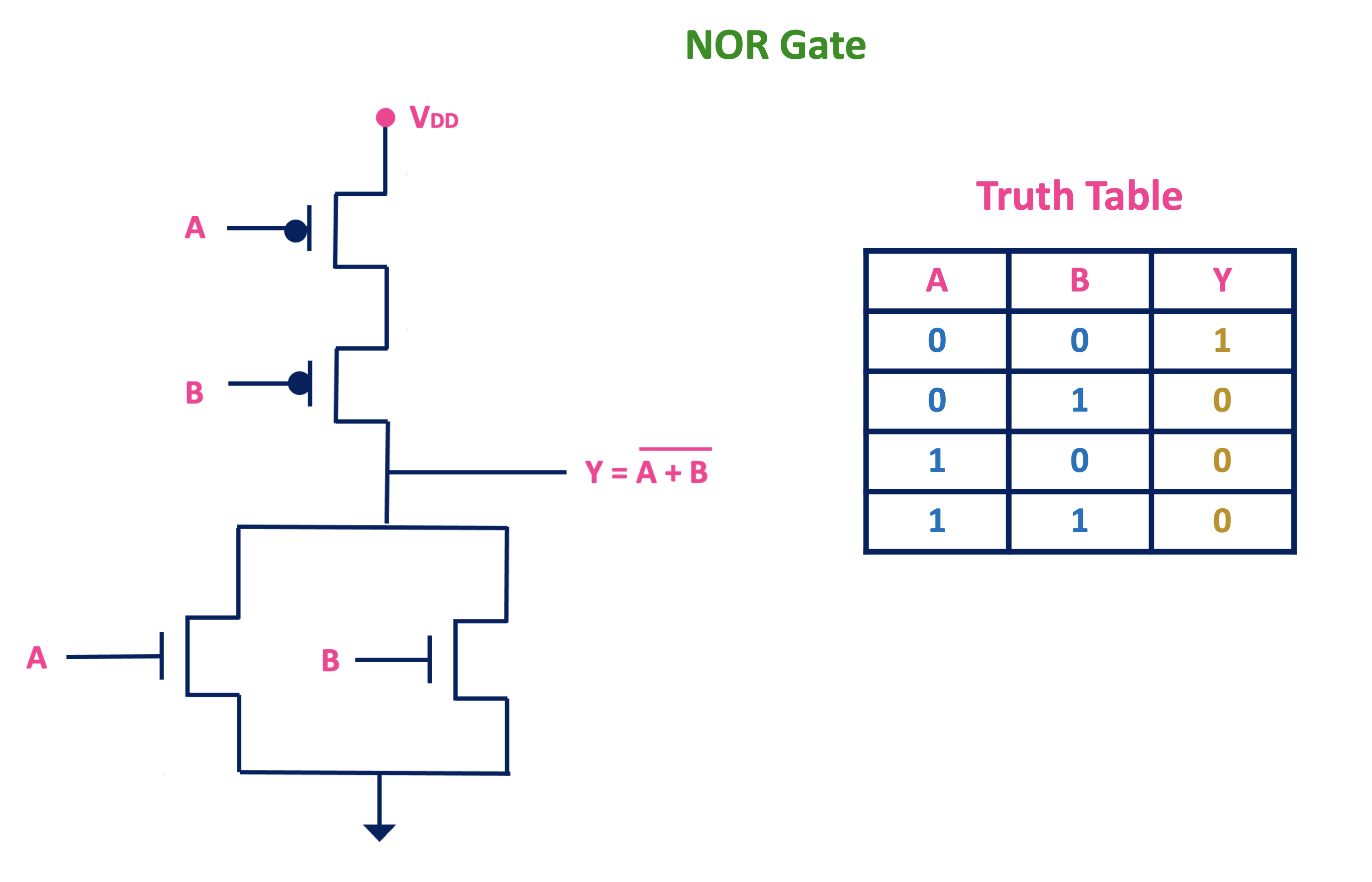
For two input NOR gate, if A and B are the inputs then its output Y = (A+B)’.
In the NMOS network, whenever there is an OR operation between the two variables then two NMOS transistors will get connected in parallel. And the output will be complement of it.
The PMOS network will be the dual of the NMOS network. Therefore, in the PMOS network, the two PMOS transistors will get connected in series.
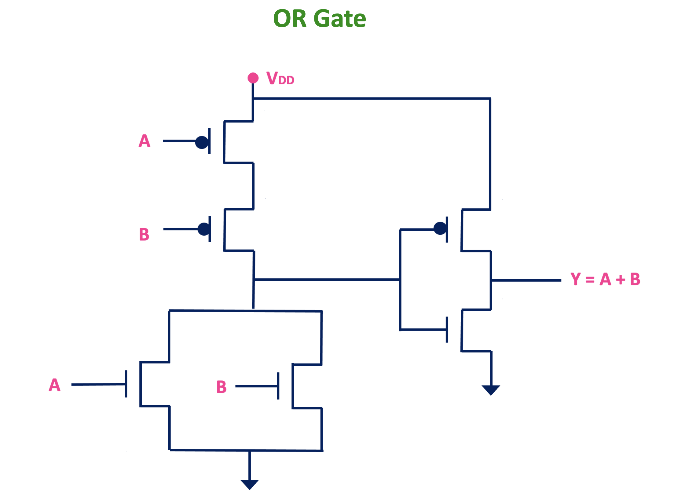
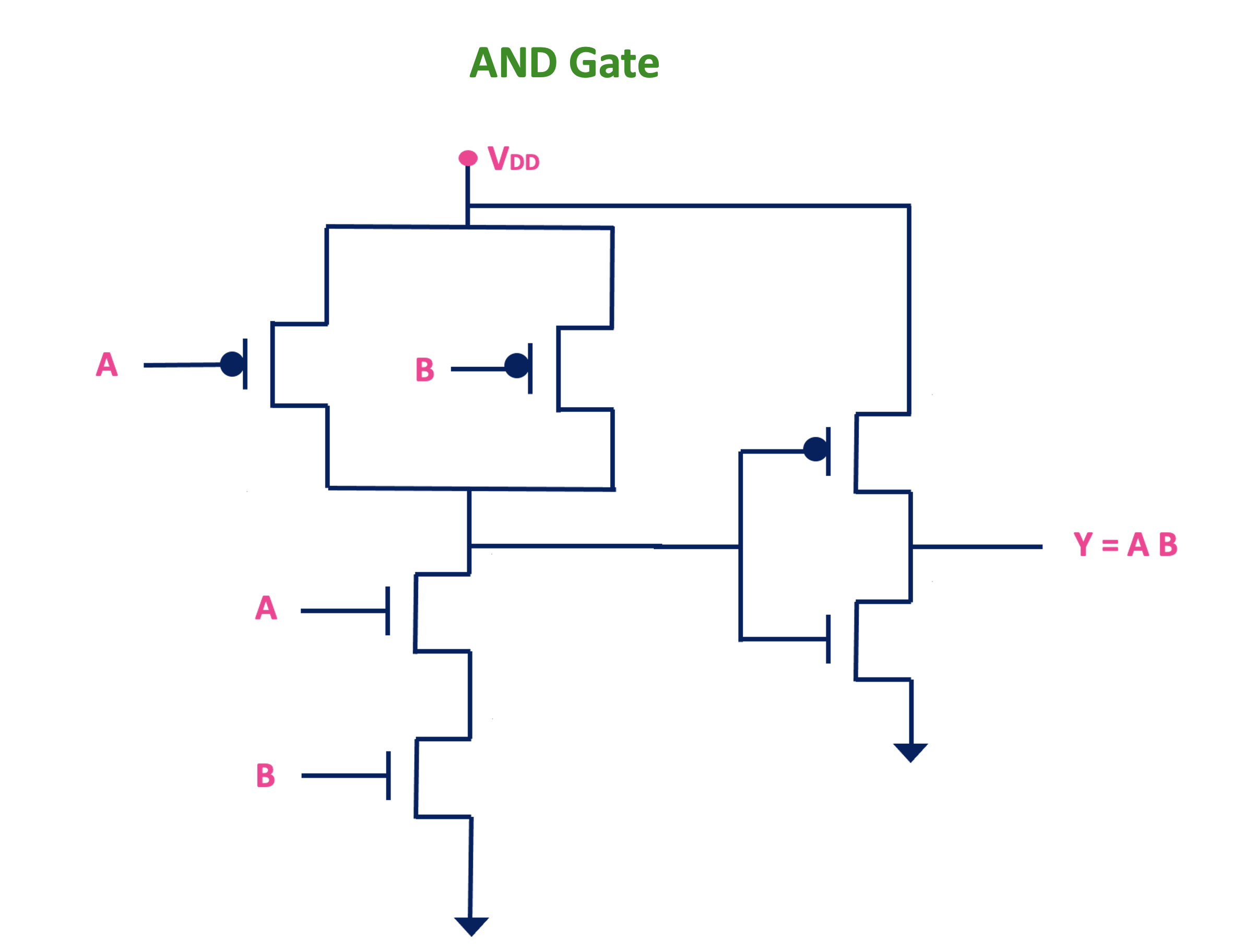
Implementation of AND and OR gate using CMOS Logic:
OR Gate:
To implement the OR gate, just add the inverter at the output of the NOR gate. The CMOS OR gate is shown below.
AND Gate :
Similarly, by connecting the inverter at the output of the NAND gate, we can implement AND gate. The CMOS AND gate is shown below.
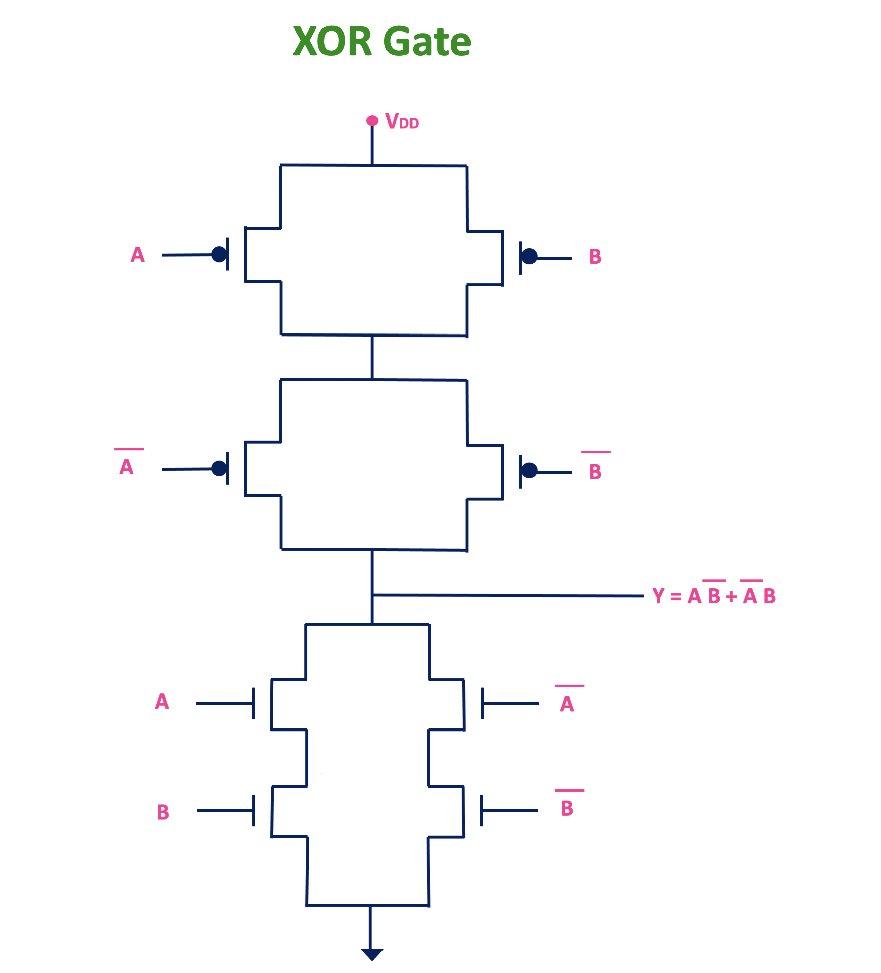
Implementation of XOR Gate and XNOR using CMOS Logic :
Similarly, the implementation of XOR and XNOR gate is shown below.
XOR Gate:
XNOR Gate :

For more information, check this video on CMOS Logic gates.
thank you
i have an assignment due in one and half hour and this saved me, thank you!
what is the difference between –>| ans –o>| in the graphs ?
–>| represents the NMOS transistors, while –o>| represents the PMOS transistors