JK Flip-Flop Symbol and Truth Table
In the SR Flip-Flop, when both inputs S and R are 1 then the output of the flip-flop is indeterminate. That issue can be resolved using the JK Flip-Flop. Similar to the SR Flip-Flop, the JK flip-flop has two inputs. And using the two inputs the flip-flop can be set, reset, hold (memory) or toggled. Unlike the SR flip-flop, in the JK flip-flop, when both inputs J and K are 1 then the output of the flip-flop toggles. The symbol of edge triggered JK flip-flop and its truth table is shown below.
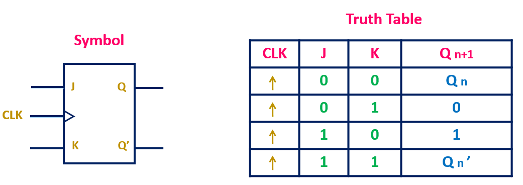
JK Flip-Flop Symbol and Truth Table
In the JK flip-flop, at the rising edge of the clock, when J = 0 and K = 0 then flip-flop retains (holds) the current state. When J = 0 and K = 1, then flop-flop resets to 0. When J = 1 and K = 0, then flip-flop sets the output to 1. And when J = 1 and K = 1 then output of the flip-flop toggles. When the clock signal is low, then irrespective of the value of J and K inputs, the flop-flop retains the present state. The detailed truth table with all different possibilities of Qn, J and K inputs are shown below, where Qn is the present state and Qn+1 is the next state of the flip-flop.
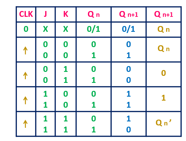
JK Flip-Flop Truth Table
The negative edge triggered JK flip-flop is similar to the positive edge triggered flip-flop. But it responds to the inputs only at the falling edge of the clock. The symbol and truth table of negative edge triggered flip-flop is shown below.

Symbol and Truth Table of Negative Edge Triggered JK Flip-Flop
JK Flip-Flop Circuit Diagram
With the little modification in the circuit of the SR flip-flop circuit, it can be used as the JK flip-flop. The circuit of JK flip-flop is shown below.
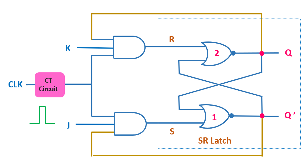
Circuit Diagram of Positive Edge Triggered JK Flip-Flop
As you can see from the circuit diagram, in the RS flip-flop circuit, the K input is applied in place of the R input while the J input is applied in place of the S input. Moreover, there is a feedback from output to input side. The Q output is connected back the AND gate where the K input is applied while the Q’ output is connected back to the AND gate where the J input is applied. Here the clock transition circuit generates the narrow pulses at the every clock transition. The same is applied to the enable input of the latch. And in this way, the gated latch behaves as an edge triggered flip-flop.
The same circuit can also be implemented using the NAND gates. The circuit diagram of the JK flip-flop with the NAND gates is shown below.
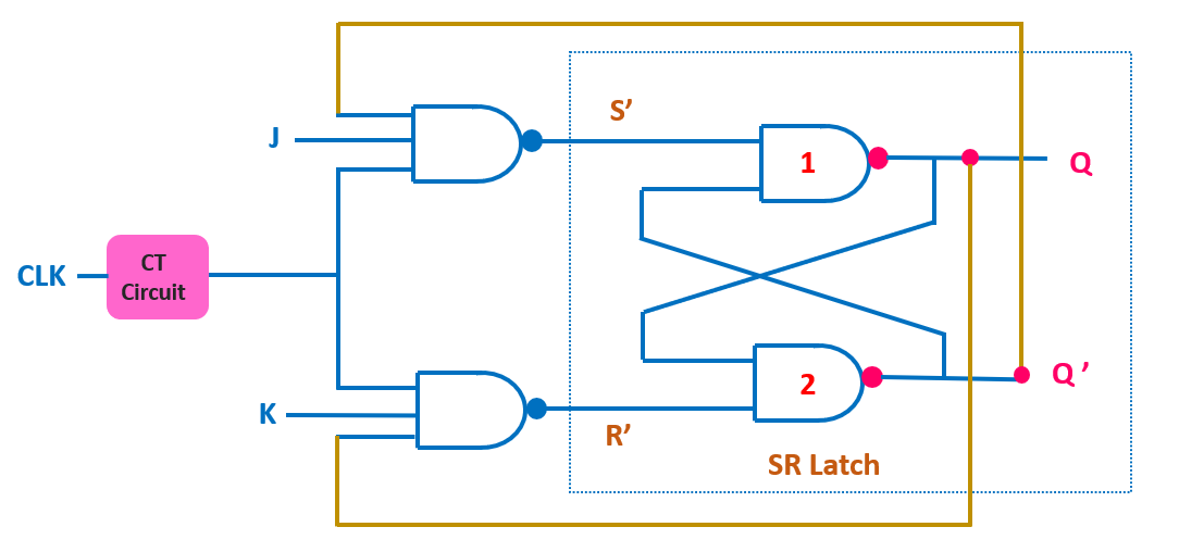
Circuit Diagram of Positive Edge Triggered JK Flip-Flop (using NAND gates)
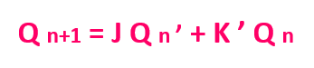
JK Flip-Flop Characteristic Equation
The characteristic equation shows the output of the flip-flop Q n+1 in terms of the present state Q n and the current inputs J and K. The characteristic table of the JK flip-flop is shown below.
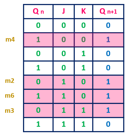
The characteristic Table of JK Flip-Flop
As per the characteristic equation, the output Q n+1 is ‘1’ for 4 different input combinations. ( 4 minterms). Using the K-map, the algebraic expression can be simplified further.
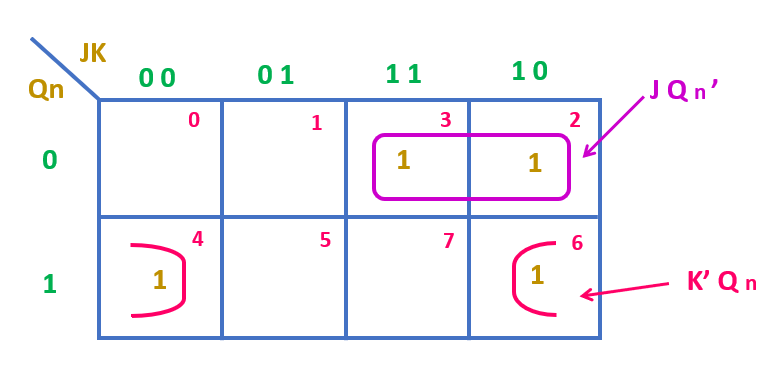
As per the K-map, after the simplification the output of the flip-flop or the characteristic equation
JK Flip-Flop Excitation Table
The excitation table of the flip-flop shows the required excitation to the flip-flop, or the required input to the flip-flop, to go from the given state to the next particular state. The excitation table of the JK flip-flop is shown below. In the table, ‘X’ represents that the value of input variable can be either ‘0’ or ‘1’.
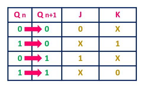
Excitation Table of JK Flip-Flop
For more information, please check the video on JK Flip-Flop
JK Flip-Flop Timing Diagram
The below timing diagram shows, how the positive edge triggered JK Flip-Flop behaves when J and K input changes with time. Since it is a positive edge triggered flip-flop, so it will respond to the inputs only at the rising edge of the clock.
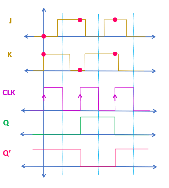
Timing Diagram of JK Flip-Flop
At the first rising edge of the clock, when J = 0 and K = 1, then output Q becomes 0 and it remains in that state until next rising edge. In between, even if the input changes, the flip-flop does not responds to the input changes.
At the second rising edge, since J = 1 and K = 0, the output of the flip-flop becomes 1. And it remains in that state until next rising edge.
At the third rising edge, since both J and K inputs are 1, the output of the flip-flop toggles and it becomes 0.
Race Around Condition in JK Flip-Flop
In the level triggered JK Flip-Flop, when J=K=1, and the ON time of the clock is more than the propagation delay of the JK Flip-Flop ,then because of the feedback from output to the input, the output of the flip-flop may toggle continuously between ‘1’ and ‘0’. This condition is known as the Race Around condition. Because of the Race Around Condition’, we cannot predict the output of the flip-flop at the end of the clock. It can be either ‘0’ or ‘1’. That’s why this Race Around Condition is undesired in the JK Flip-Flop. The issue of Race Around Condition can be resolved using the Master-Slave Flip-Flop. The below diagram shows the Race Around Condition in the JK Flip-Flop.
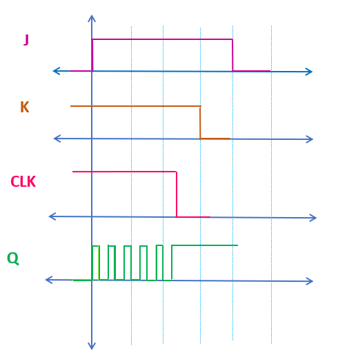
Race Around Condition in the JK Flip-Flop